首页 > 英联产品 > 分立器件 > 带TVS阵列的EMI滤波器 > CLC类EMI滤波器
UM8511
具有集成ESD保护的8线LC类EMI滤波器
Datasheet Reliability Report Package Information Order Sample  
Key Specifications
Part Number Description Status SubFamily Transient Standards L (nH) R (Ohm) C (pF), VR=2#5V Attenuation @ 800 MHz (db) Attenuation @ 2#5 GHz (db) VRWM MAX (V) IR MAX at VRWM uA at 25°C VBR MIN (V) CTOT MAX (pF) L-G Lines: Uni-directional Protection Lines: Bi-directional Protection Pin/Package EV Kit Available?
UM8511 具有集成ESD保护的8线LC类EMI滤波器 ACTIVE CLC Filter IEC 61000-4-2 17 10 12 -22 -45 5 0.1 6 24 8 0 16/DFN 3.3×1.3 Y
View All>>

Product Description  

The UM8511 is a (L-C) low pass filter array with integrated TVS diodes. It is designed to suppress unwanted EMI signals and provide electrostatic discharge (ESD) protection in portable electronic equipment. This device utilizes solid-state silicon-avalanche technology for superior clamp­ing performance and DC electrical characteristics. It has been optimized for protection of signal lines in cellular phones and other portable electronics.
The device consists of identical circuits comprised of TVS diodes for ESD protection, and a C-L-C network for EMI filtering. A typical inductor value of 17nH and a capacitor value of 12pF are used to achieve 19dB minimum attenuation from 800MHz to 2.7GHz. The TVS diodes provide effective suppression of ESD voltages in excess of ±15kV (air discharge) and ±8kV (contact discharge) per IEC 61000-4-2, level 4.
The UM8511 is in a RoHS compli­ant DFN16 3.3×1.3 package. The leads are finished with lead-free. The small pack­age makes it ideal for use in portable electronics such as cell phones, digital still cameras, and PDAs.
 
Features
 
- Bidirectional EMI Filter with Integrated TVS for ESD Protection
- ESD Protection to IEC 61000-4-2 (ESD) Level 4, ±15kV (Air), ±8kV (Contact)
- Filter Performance: 19dB Minimum Attenuation from 800MHz to 2.7GHz
- TVS Working Voltage: 5V
- Inductor: 17nH (Typical)
- Capacitors: 12pF (Typical at VR=2.5V)
- Protection and Filtering for Multi Lines
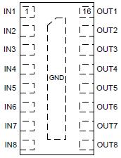
  UM8511: Eight Lines
 
Applications
 
- Signal Lines Protection
- Cell Phone CCD Camera Lines
- Clamshell Cell Phones
 
Pin Configurations  

                                                         
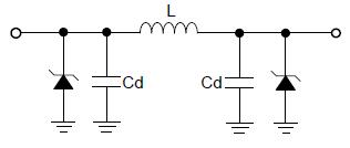
          UM8511 Top View                                                                                  Device Schematic (8X)
 
Electrical Characteristics (TJ=25°C, unless otherwise noted)

Parameter
Symbol
Conditions
Min
Typ
Max
Unit
TVS Reverse Stand-Off Voltage
VRWM


5
V
TVS Reverse Breakdown Voltage
VBR
 IT=1mA
6
8
10
V
TVS Reverse Leakage Current
IR
 VRWM=3.3V
 
 
0.1
μA
DC Resistance
Rcc
 
 
10
 
Ω
Filter Cut-Off Frequency
fc
Zsource=Zload=50Ω
 
250
 
MHZ
Inductance
L
 
 
17
 
nH
Capacitance
Cd
VR=2.5V, f=1MHz
 
12
 
pF
Total Capacitance
Ctotal
Input to GND,
Each Line
VR=2.5V, f=1MHz
 
19
24
 
29
pF
Stop Band Attenuation
 
800MHz to 2.7GHz
 
19
 
dB
   
Ordering Information

Part Number
Working Voltage
Packaging Type
Channel
Marking Code
Shipping Qty
UM8511
5.0V
DFN16 3.3×1.3
8
8511
3000pcs/7Inch
Tape & Reel
  
Application Notes
微处理器超长启动周期中的外部看门狗管理方案v2.pdf
利用3.3V供电RS485接口实现远距离数据通信.pdf
高速低电源电压逻辑电平转换电路.pdf
超低功耗LDO线性稳压器.pdf
I2C-BUS电平转换芯片在安防产品的应用.pdf
0201超小封装ESD保护器件.pdf
Analog Switch Permits Port Sharing in Portable Equipment.pdf
Balanced Modulator Demodulator Employing UM4684.pdf
Level Shifter for High Speed and Wide Voltage Range Interface.pdf
Low Resistance Analog Switches Permit Speaker Switching in Audio Devices.pdf
Low-Icct Analog Switches for Ultra-Portable Designs.pdf
Selecting the Right CMOS Analog Switch.pdf
Product Selection Guide
ESD Protection and EMI Filters Selection Guide.pdf
Product Search
Parametric Search
Product You Recently Viewed
@2014 Union Semiconductor Limited. All rights Reserved.
FOLLOW US